OmniVision expands TheiaCel sensor portfolio
OmniVision announced several new sensors at AutoSens Europe 2024 featuring TheiaCel technology.
OX12A10 12-megapixel (MP)-resolution CMOS image sensor
The OX12A10 improves automotive safety by providing enhanced resolution and image quality, regardless of lighting conditions. The OX12A10 is ideal for high-performance front machine vision cameras for advanced driver assistance systems (ADAS) and autonomous driving (AD).
The 12MP OX12A10 is the highest-resolution sensor in OMNIVISION’s 2.1-micron (µm) TheiaCel product family, which also includes the 8MP OX08D10 and 5MP OX05D10 devices. TheiaCel harnesses the capabilities of next-generation lateral overflow integration capacitors (LOFIC) and OMNIVISION’s DCG high dynamic range (HDR) technology to eliminate LED flicker regardless of lighting conditions. OMNIVISION’s TheiaCel solution also achieves a wider dynamic range than earlier automotive HDR architectures.
“OMNIVISION sensing solutions provide increased driving safety and autonomy, and our new OX12A10 brings all of the most important features together into a single device, including high resolution, excellent low-light performance, LED flicker mitigation (LFM), small size, power efficiency and best-in-class high-temperature performance,” said Dr. Paul Wu, head of automotive product marketing, OMNIVISION. “Initially launched to the market at AutoSens last year, our TheiaCel™ technology has attracted great interest, and we are excited to round out the product family with the first high-performance 12MP sensor for the automotive industry. Our 5MP and 8MP solutions are designed for mainstream passenger vehicles, while the OX12A10 is designed to meet next-generation ADAS and AD machine vision requirements.”
The OX12A10 has a 1/1.43-inch optical format and is the first image sensor to feature OMNIVISION’s a-CSP+ package technology. At just 12450µm x 8100µm in size, it has a much more compact design than traditional ball grid array (BGA) packages.
The OX12A10 is available for sampling now and will be in mass production in Q3 2025.
3-megapixel (MP)-resolution OX03H10 CMOS image sensor
The second is a 3.0-micron (µm) pixel automotive viewing sensor with TheiaCel technology. Announced at AutoSens Europe 2024, the new solution significantly enhances driving safety by enabling imaging clarity in all lighting conditions for surround-view and rear-view cameras.
“The OX03H10 image sensor has excellent low-light performance and shows unrivalled LED flicker mitigation (LFM) by utilizing a single exposure to generate the entire 140 dB dynamic range. This is achieved using our TheiaCel technology, which harnesses the capabilities of lateral overflow integration capacitor (LOFIC) technology, together with OMNIVISION’s proprietary single-exposure DCG and our well known split pixel high dynamic range (HDR) technology, to enable superior image quality regardless of lighting conditions,” said Naresh Shetty, automotive product marketing manager, OMNIVISION. “We are excited to launch the OX03H10 for cameras across all next-generation automotive classes to improve visibility for every aspect of driving and vehicle ownership.”
At 1920 x 1536 resolution, the OX03H10 features 60 frames per second (fps) and has low power consumption. The 3.0-µm pixel is based on PureCelPlus-S stacking technology for the smallest pixel and highest resolution in a 1/2.44-inch optical format. It comes in a small a-CSP package size and is pin-to-pin compatible with OMNIVISION’s OX03F10 automotive image sensor for seamless upgrades. The OX03H10 meets ASIL-C functional safety regulations, features cybersecurity and has a MIPI output interface.
The OX03H10 is available for sampling now and will be in mass production in the first half of 2025.
Back-side illuminated (BSI) global shutter (GS) image sensor
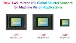
The company also announced three new back-side illuminated (BSI) global shutter (GS) image sensors for machine vision applications including industrial automation, robotics, logistics barcode scanners and intelligent transportation systems (ITS).
The new GS image sensors feature a 3.45-micron (µm) BSI pixel for high sensitivity, shutter efficiency and excellent low-light performance. Their advanced performance in a smaller pixel enables them to replace larger 4.8 µm pixel front-side illuminated (FSI) sensors traditionally used in machine vision products.
“OMNIVISION is the leader in high-performance BSI GS sensors for the machine vision industry with a product portfolio that features 3.45 µm and 2.2 µm pixel solutions with resolutions ranging from 2- to 9-megapixel (MP),” said Kelly Yan, staff marketing manager, OMNIVISION. “Our patented technologies enable us to deliver higher image quality and better performance in a compact design to improve high-speed image capture, with higher SNR (Signal noise ratio) and improved accuracy.”
New sensor technologies include:
- An advanced PureCelPlus-S stacked-die architecture enables thinner modules with best-in-class light absorption, enhanced image quality from heightened sensitivity, and a large angular response that prevents color shading issues.
- Nyxel near-infrared (NIR) technology, which boosts quantum efficiency (QE) at 700-1050nm, enabling the capture of brighter images from farther away.
- Small 3.45 µm pixels that achieve high shutter efficiency at 106dB.
- 20Ke- full-well capacity (FWC), enabling higher high dynamic range (HDR) with low noise level, resulting in clearer pictures.
- On-chip dual conversion gain (DCG) HDR to extend dynamic range, reproducing motion artifact–free and low-noise images in challenging lighting conditions.
Three new sensors for machine vision applications:
- The OG02C10/1B: 2MP BSI GS sensor in a 1/2.53-inch optical format (OF) that supports 300 frames per second (fps)
- The OG03A10/1B: 3MP BSI GS sensor in a 1/1.8-inch OF that supports 150 fps
- The OG05C10/1B: 5MP BSI GS sensor in a 1/1.45-inch OF that supports 120 fps
All of the new GS sensors fit the standard C-mount lens and provide support for both LVDS and MIPI interfaces. The 3.45 µm BSI GS sensor family also includes the OG09A10, a 9MP BSI GS sensor in a 1-inch OF. The 2.2 µm BSI GS sensor family includes the OG05B1B, a 5MP resolution sensor in a 1/2.53-inch OF, and the OG01H1B, a 1.5MP resolution GS sensor in a 1/4.51-inch OF.
The OG03A10/1B and OG05C10/1B sensors are available for sampling now and are already in mass production. The OG02C10/1B sensor will be available for sampling in Q1 2025 and in mass production in 2H 2025.


